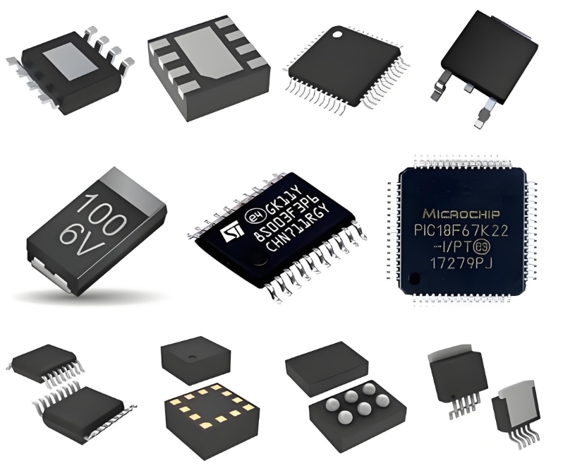
Microchip TC4426EOA Dual High-Speed Power MOSFET Driver: Datasheet, Application Circuit, and Design Considerations
The efficient and reliable switching of power MOSFETs and IGBTs is a cornerstone of modern power electronics, found in applications ranging from motor controllers and switch-mode power supplies (SMPS) to inverters and Class-D amplifiers. The Microchip TC4426EOA is a pivotal component designed specifically to meet this challenge. As a dual high-speed, high-current MOSFET driver, it provides the necessary interface between low-power control circuits (like MCUs or PWM controllers) and the high-power switching devices that do the heavy lifting.
This article delves into the key specifications of the TC4426EOA, explores a typical application circuit, and outlines critical design considerations for maximizing performance.
Datasheet Highlights and Key Specifications
The TC4426EOA datasheet reveals a robust and versatile driver IC. Its primary function is to amplify a low-current logic signal into a high-current output capable of rapidly charging and discharging the highly capacitive gate of a power MOSFET. Key specifications that define its performance include:
High Peak Output Current: With the ability to source and sink 1.5A of peak current, the TC4426 can switch large gate charges very quickly, minimizing transition times and associated switching losses.
High-Speed Operation: It features fast rise and fall times (typically < 25 ns into a 1,000 pF load), which is essential for high-frequency switching applications to maintain efficiency.
Dual Independent Channels: The IC contains two identical drivers, which can be used independently to control two separate switches or combined in parallel to effectively double the available drive current (to approximately 3A).
Wide Operating Voltage Range (4.5V to 18V): This flexibility allows it to interface with various logic families (e.g., 5V TTL/CMOS) and directly drive MOSFETs with gate thresholds ranging from standard to logic-level.
Low Output Impedance: A typical output impedance of 7Ω ensures a strong, low-impedance drive, which helps prevent gate oscillations and ensures crisp switching.
Latch-Up Protected: The design is immune to latch-up, enhancing reliability in demanding environments.
Package: It is offered in an 8-pin SOIC package, making it suitable for space-constrained PCB designs.
Typical Application Circuit
A standard application circuit for one channel of the TC4426EOA is straightforward but requires careful attention to component placement. The core circuit involves:
1. Power Supply Decoupling: A low-ESR (Equivalent Series Resistance) decoupling capacitor, typically a 1µF to 10µF ceramic capacitor placed as close as possible to the Vdd and GND pins of the IC, is absolutely critical. This capacitor provides the instantaneous current needed during the switching events.

2. Input Signal: The input pin, which is TTL/CMOS compatible, is connected to the source of the control signal (e.g., a microcontroller's PWM output pin). A small series resistor (e.g., 10-100Ω) can sometimes be added to dampen any ringing on the input line.
3. Output to MOSFET Gate: The output pin is connected directly to the gate of the power MOSFET. A series gate resistor (Rg) is almost always used between the driver output and the MOSFET gate. This resistor serves multiple purposes: it controls the switching speed (trade-off between speed and EMI), dampens high-frequency oscillations caused by parasitic inductance and the MOSFET's gate capacitance, and can limit peak current in the driver.
Critical Design Considerations
To ensure robust and efficient operation, several factors must be considered during the design phase:
Gate Resistor Selection: The value of Rg is a crucial tuning parameter. A lower value allows faster switching but increases EMI and current stress on the driver. A higher value reduces noise and overshoot but increases switching losses. The optimal value is often found through prototyping and measurement.
Layout Parasitics: PCB layout is paramount in high-speed switching circuits. The loop formed by the decoupling capacitor, the driver IC, and the power MOSFET must be as small as possible to minimize parasitic inductance. Excessive inductance can cause severe voltage spikes, ringing, and even damage the driver or MOSFET.
Power Dissipation and Thermal Management: The power dissipated by the driver is related to the switching frequency and the total gate charge of the MOSFET. For high-frequency operations or when driving large MOSFETs, it is essential to calculate the power dissipation and ensure the IC's junction temperature remains within safe limits. The small SOIC package relies on a well-designed PCB ground plane for heat dissipation.
Using Channels in Parallel: For driving a single very large MOSFET or parallel MOSFETs, the two channels can be connected in parallel to increase drive strength. This requires connecting the respective inputs together and the respective outputs together, typically with a small series resistor in each output path to prevent current imbalances between the two channels.
The Microchip TC4426EOA is an exceptionally versatile and robust solution for driving power MOSFETs and IGBTs. Its high-speed switching capability, substantial peak current output, and dual-channel architecture make it suitable for a vast array of power conversion and control applications. Success hinges not only on understanding its electrical specifications but also on implementing a careful board layout and selecting appropriate external components like the gate resistor and decoupling capacitors.
Keywords:
1. MOSFET Driver
2. High-Current
3. Gate Charge
4. Switching Losses
5. PCB Layout
