
Onsemi MUN5214T1G Digital Transistor: Features, Applications, and Circuit Design Considerations
The Onsemi MUN5214T1G represents a fundamental yet highly efficient class of components: the digital transistor. This device integrates a single NPN bipolar junction transistor (BJT) with a monolithic bias resistor network, combining two passive components into a single package. This integration simplifies circuit design, reduces the component count on a PCB, and enhances overall system reliability. It is specifically designed for the interface between low-power digital circuits (like MCUs or FPGAs) and higher-current loads.
Key Features
The MUN5214T1G is characterized by several critical features that make it a preferred choice for designers:
Integrated Resistor Network: The device includes a series base resistor (R1 = 10 kΩ) and a base-emitter resistor (R2 = 10 kΩ). This eliminates the need for external discrete resistors, saving board space and assembly costs.
High DC Current Gain: It offers a minimum DC current gain (hFE) of 100 at 10 mA, ensuring effective signal amplification with very low input current requirements.
Low Saturation Voltage: With a collector-emitter saturation voltage (VCE(sat)) typically around 100 mV, it minimizes power loss when switched fully on, improving energy efficiency.
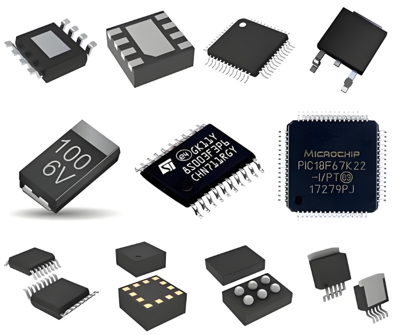
Small Footprint: Housed in a SOT-23-3 surface-mount package, it is ideal for space-constrained modern electronic applications.
Simplified Drive Logic: It can be directly driven from 3.3V or 5V microcontroller GPIO pins, making it an ideal interface solution.
Primary Applications
The integration and characteristics of the MUN5214T1G make it suitable for a wide array of applications, including:
Load Switching: Driving relays, solenoids, LEDs, and DC motors.
Logic Level Inversion: Acting as an inverter in digital circuits.
Input Buffering: Isolating and conditioning signals for microcontrollers.
Automotive and Industrial Systems: Used in body control modules, sensor interfaces, and power management systems due to its robustness.
Critical Circuit Design Considerations
While the MUN5214T1G simplifies design, several factors must be considered for optimal performance:
1. Input Current Calculation: The integrated resistors dictate the required input drive current. The formula I_IN ≈ (V_GPIO - V_BE) / R1 is crucial. For a 3.3V GPIO (assuming V_BE = 0.7V), the input current is approximately (3.3V - 0.7V) / 10 kΩ = 260 µA, which is well within the capabilities of any modern microcontroller.
2. Load Current Limitations: The absolute maximum collector current (IC) is 100 mA. Designers must ensure the continuous and peak currents of the connected load do not exceed this rating to prevent device failure.
3. Switching Speed and Miller Capacitance: For high-frequency switching applications, the inherent capacitance of the BJT can limit performance. While adequate for many DC and low-frequency switches (up to 100kHz), it is not optimized for high-speed (MHz) switching like a MOSFET would be.
4. Power Dissipation: The total power dissipated by the device (Ptot) must not exceed the specified maximum of 250 mW. This is calculated as the sum of the power dissipated in the collector junction and the integrated base network.
5. Flyback Diode for Inductive Loads: When driving inductive loads such as relays or motors, an external flyback diode must be placed across the load to suppress voltage spikes generated when the current is suddenly interrupted, protecting the transistor from damage.
In summary, the Onsemi MUN5214T1G digital transistor is an exceptionally useful component for simplifying and improving the reliability of digital interface circuits. Its built-in bias network allows for direct connection to microcontroller GPIOs, making it a go-to solution for designers looking to drive moderate-current loads efficiently and save valuable PCB space. It is a quintessential part for any design engineer's toolkit when a simple, reliable, and cost-effective switching solution is required.
Keywords: Digital Transistor, NPN BJT, GPIO Interface, Load Switching, SOT-23

